
1. Crystal Framework and Polytypism of Silicon Carbide
1.1 Cubic and Hexagonal Polytypes: From 3C to 6H and Beyond
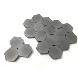
(Silicon Carbide Ceramics)
Silicon carbide (SiC) is a covalently bonded ceramic composed of silicon and carbon atoms arranged in a tetrahedral control, forming among the most intricate systems of polytypism in products scientific research.
Unlike a lot of porcelains with a solitary steady crystal structure, SiC exists in over 250 recognized polytypes– distinct stacking series of close-packed Si-C bilayers along the c-axis– ranging from cubic 3C-SiC (additionally referred to as β-SiC) to hexagonal 6H-SiC and rhombohedral 15R-SiC.
One of the most usual polytypes used in engineering applications are 3C (cubic), 4H, and 6H (both hexagonal), each showing slightly different electronic band structures and thermal conductivities.
3C-SiC, with its zinc blende framework, has the narrowest bandgap (~ 2.3 eV) and is normally expanded on silicon substrates for semiconductor tools, while 4H-SiC provides exceptional electron mobility and is liked for high-power electronic devices.
The solid covalent bonding and directional nature of the Si– C bond provide remarkable solidity, thermal stability, and resistance to sneak and chemical assault, making SiC suitable for severe atmosphere applications.
1.2 Issues, Doping, and Digital Characteristic
Regardless of its architectural intricacy, SiC can be doped to attain both n-type and p-type conductivity, allowing its use in semiconductor tools.
Nitrogen and phosphorus function as benefactor impurities, introducing electrons right into the transmission band, while light weight aluminum and boron work as acceptors, developing openings in the valence band.
However, p-type doping efficiency is limited by high activation powers, particularly in 4H-SiC, which positions obstacles for bipolar gadget style.
Native problems such as screw misplacements, micropipes, and piling faults can deteriorate device performance by working as recombination facilities or leakage paths, requiring high-quality single-crystal growth for electronic applications.
The vast bandgap (2.3– 3.3 eV depending upon polytype), high failure electrical field (~ 3 MV/cm), and exceptional thermal conductivity (~ 3– 4 W/m · K for 4H-SiC) make SiC much superior to silicon in high-temperature, high-voltage, and high-frequency power electronics.
2. Processing and Microstructural Engineering
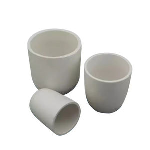
( Silicon Carbide Ceramics)
2.1 Sintering and Densification Techniques
Silicon carbide is naturally challenging to densify due to its solid covalent bonding and reduced self-diffusion coefficients, requiring sophisticated processing methods to accomplish complete thickness without additives or with marginal sintering aids.
Pressureless sintering of submicron SiC powders is feasible with the addition of boron and carbon, which advertise densification by eliminating oxide layers and enhancing solid-state diffusion.
Hot pushing uses uniaxial stress throughout home heating, enabling full densification at reduced temperature levels (~ 1800– 2000 ° C )and creating fine-grained, high-strength components ideal for cutting tools and wear components.
For huge or complicated forms, reaction bonding is employed, where porous carbon preforms are infiltrated with liquified silicon at ~ 1600 ° C, creating β-SiC in situ with marginal shrinkage.
Nevertheless, residual free silicon (~ 5– 10%) remains in the microstructure, restricting high-temperature efficiency and oxidation resistance above 1300 ° C.
2.2 Additive Production and Near-Net-Shape Manufacture
Recent breakthroughs in additive manufacturing (AM), particularly binder jetting and stereolithography utilizing SiC powders or preceramic polymers, make it possible for the fabrication of complicated geometries formerly unattainable with standard approaches.
In polymer-derived ceramic (PDC) paths, fluid SiC forerunners are shaped by means of 3D printing and then pyrolyzed at high temperatures to produce amorphous or nanocrystalline SiC, frequently needing further densification.
These methods minimize machining expenses and product waste, making SiC much more accessible for aerospace, nuclear, and warmth exchanger applications where elaborate styles boost efficiency.
Post-processing steps such as chemical vapor seepage (CVI) or fluid silicon infiltration (LSI) are sometimes made use of to boost thickness and mechanical honesty.
3. Mechanical, Thermal, and Environmental Performance
3.1 Toughness, Hardness, and Wear Resistance
Silicon carbide ranks amongst the hardest recognized products, with a Mohs solidity of ~ 9.5 and Vickers hardness going beyond 25 GPa, making it extremely immune to abrasion, disintegration, and scratching.
Its flexural toughness usually varies from 300 to 600 MPa, depending upon processing approach and grain dimension, and it maintains toughness at temperature levels up to 1400 ° C in inert atmospheres.
Crack sturdiness, while moderate (~ 3– 4 MPa · m 1ST/ ²), suffices for numerous structural applications, particularly when integrated with fiber reinforcement in ceramic matrix compounds (CMCs).
SiC-based CMCs are made use of in generator blades, combustor liners, and brake systems, where they provide weight cost savings, fuel efficiency, and expanded service life over metal equivalents.
Its outstanding wear resistance makes SiC ideal for seals, bearings, pump parts, and ballistic shield, where resilience under extreme mechanical loading is crucial.
3.2 Thermal Conductivity and Oxidation Stability
Among SiC’s most important homes is its high thermal conductivity– approximately 490 W/m · K for single-crystal 4H-SiC and ~ 30– 120 W/m · K for polycrystalline forms– exceeding that of lots of steels and making it possible for effective warm dissipation.
This residential or commercial property is important in power electronic devices, where SiC gadgets produce much less waste heat and can operate at greater power densities than silicon-based gadgets.
At elevated temperatures in oxidizing environments, SiC creates a safety silica (SiO TWO) layer that slows additional oxidation, giving great environmental sturdiness as much as ~ 1600 ° C.
Nevertheless, in water vapor-rich settings, this layer can volatilize as Si(OH)FOUR, resulting in sped up degradation– a crucial challenge in gas generator applications.
4. Advanced Applications in Energy, Electronics, and Aerospace
4.1 Power Electronic Devices and Semiconductor Devices
Silicon carbide has changed power electronics by allowing gadgets such as Schottky diodes, MOSFETs, and JFETs that run at greater voltages, regularities, and temperatures than silicon matchings.
These devices minimize power losses in electric automobiles, renewable resource inverters, and industrial motor drives, contributing to worldwide power effectiveness enhancements.
The capacity to operate at joint temperature levels above 200 ° C enables streamlined air conditioning systems and enhanced system integrity.
Additionally, SiC wafers are utilized as substratums for gallium nitride (GaN) epitaxy in high-electron-mobility transistors (HEMTs), integrating the advantages of both wide-bandgap semiconductors.
4.2 Nuclear, Aerospace, and Optical Systems
In nuclear reactors, SiC is a crucial part of accident-tolerant fuel cladding, where its reduced neutron absorption cross-section, radiation resistance, and high-temperature toughness improve security and efficiency.
In aerospace, SiC fiber-reinforced compounds are used in jet engines and hypersonic vehicles for their light-weight and thermal stability.
In addition, ultra-smooth SiC mirrors are employed precede telescopes as a result of their high stiffness-to-density proportion, thermal security, and polishability to sub-nanometer roughness.
In recap, silicon carbide ceramics stand for a cornerstone of modern-day sophisticated products, incorporating extraordinary mechanical, thermal, and electronic buildings.
Via accurate control of polytype, microstructure, and processing, SiC remains to make it possible for technical developments in power, transport, and extreme environment engineering.
5. Supplier
TRUNNANO is a supplier of Spherical Tungsten Powder with over 12 years of experience in nano-building energy conservation and nanotechnology development. It accepts payment via Credit Card, T/T, West Union and Paypal. Trunnano will ship the goods to customers overseas through FedEx, DHL, by air, or by sea. If you want to know more about Spherical Tungsten Powder, please feel free to contact us and send an inquiry(sales5@nanotrun.com).
Tags: silicon carbide ceramic,silicon carbide ceramic products, industry ceramic
All articles and pictures are from the Internet. If there are any copyright issues, please contact us in time to delete.
Inquiry us