

1. Crystal Structure and Split Anisotropy
1.1 The 2H and 1T Polymorphs: Architectural and Electronic Duality
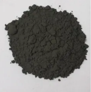
(Molybdenum Disulfide)
Molybdenum disulfide (MoS ₂) is a split change steel dichalcogenide (TMD) with a chemical formula containing one molybdenum atom sandwiched in between 2 sulfur atoms in a trigonal prismatic sychronisation, developing covalently bound S– Mo– S sheets.
These specific monolayers are piled up and down and held together by weak van der Waals pressures, making it possible for very easy interlayer shear and exfoliation down to atomically slim two-dimensional (2D) crystals– a structural attribute main to its varied useful roles.
MoS two exists in numerous polymorphic forms, the most thermodynamically stable being the semiconducting 2H stage (hexagonal balance), where each layer exhibits a direct bandgap of ~ 1.8 eV in monolayer type that transitions to an indirect bandgap (~ 1.3 eV) in bulk, a sensation crucial for optoelectronic applications.
On the other hand, the metastable 1T phase (tetragonal symmetry) takes on an octahedral sychronisation and acts as a metal conductor due to electron donation from the sulfur atoms, allowing applications in electrocatalysis and conductive compounds.
Phase changes in between 2H and 1T can be induced chemically, electrochemically, or via strain design, supplying a tunable platform for developing multifunctional gadgets.
The capacity to support and pattern these stages spatially within a single flake opens up pathways for in-plane heterostructures with distinct electronic domains.
1.2 Flaws, Doping, and Edge States
The performance of MoS two in catalytic and digital applications is extremely conscious atomic-scale defects and dopants.
Inherent factor problems such as sulfur jobs serve as electron contributors, increasing n-type conductivity and working as active websites for hydrogen development responses (HER) in water splitting.
Grain borders and line problems can either impede cost transport or develop localized conductive pathways, depending on their atomic configuration.
Controlled doping with change metals (e.g., Re, Nb) or chalcogens (e.g., Se) allows fine-tuning of the band framework, carrier concentration, and spin-orbit coupling impacts.
Notably, the edges of MoS ₂ nanosheets, specifically the metal Mo-terminated (10– 10) edges, display substantially higher catalytic task than the inert basic aircraft, motivating the design of nanostructured catalysts with taken full advantage of edge exposure.
( Molybdenum Disulfide)
These defect-engineered systems exhibit how atomic-level control can transform a naturally happening mineral into a high-performance practical product.
2. Synthesis and Nanofabrication Methods
2.1 Mass and Thin-Film Manufacturing Approaches
All-natural molybdenite, the mineral type of MoS TWO, has actually been used for years as a solid lubricating substance, yet modern-day applications demand high-purity, structurally managed artificial kinds.
Chemical vapor deposition (CVD) is the dominant method for generating large-area, high-crystallinity monolayer and few-layer MoS ₂ movies on substratums such as SiO ₂/ Si, sapphire, or versatile polymers.
In CVD, molybdenum and sulfur forerunners (e.g., MoO three and S powder) are vaporized at high temperatures (700– 1000 ° C )under controlled ambiences, allowing layer-by-layer growth with tunable domain dimension and alignment.
Mechanical exfoliation (“scotch tape technique”) stays a benchmark for research-grade examples, producing ultra-clean monolayers with minimal problems, though it does not have scalability.
Liquid-phase exfoliation, entailing sonication or shear blending of bulk crystals in solvents or surfactant solutions, produces colloidal diffusions of few-layer nanosheets suitable for finishes, compounds, and ink solutions.
2.2 Heterostructure Assimilation and Tool Pattern
The true possibility of MoS ₂ emerges when incorporated into upright or side heterostructures with other 2D products such as graphene, hexagonal boron nitride (h-BN), or WSe ₂.
These van der Waals heterostructures enable the style of atomically exact tools, including tunneling transistors, photodetectors, and light-emitting diodes (LEDs), where interlayer cost and energy transfer can be engineered.
Lithographic pattern and etching strategies allow the construction of nanoribbons, quantum dots, and field-effect transistors (FETs) with network lengths to 10s of nanometers.
Dielectric encapsulation with h-BN shields MoS ₂ from environmental degradation and reduces charge scattering, significantly boosting service provider movement and tool stability.
These fabrication advances are necessary for transitioning MoS two from laboratory curiosity to sensible part in next-generation nanoelectronics.
3. Useful Residences and Physical Mechanisms
3.1 Tribological Habits and Solid Lubrication
Among the earliest and most long-lasting applications of MoS ₂ is as a dry strong lubricant in extreme settings where liquid oils stop working– such as vacuum, heats, or cryogenic conditions.
The low interlayer shear toughness of the van der Waals space permits simple sliding in between S– Mo– S layers, resulting in a coefficient of friction as low as 0.03– 0.06 under optimal conditions.
Its performance is even more boosted by solid attachment to steel surfaces and resistance to oxidation as much as ~ 350 ° C in air, past which MoO ₃ development enhances wear.
MoS ₂ is widely utilized in aerospace systems, air pump, and firearm components, typically applied as a finish through burnishing, sputtering, or composite incorporation right into polymer matrices.
Current researches show that humidity can degrade lubricity by enhancing interlayer adhesion, prompting research right into hydrophobic finishings or hybrid lubricants for improved environmental stability.
3.2 Electronic and Optoelectronic Response
As a direct-gap semiconductor in monolayer type, MoS ₂ shows strong light-matter communication, with absorption coefficients surpassing 10 ⁵ cm ⁻¹ and high quantum yield in photoluminescence.
This makes it excellent for ultrathin photodetectors with fast feedback times and broadband level of sensitivity, from visible to near-infrared wavelengths.
Field-effect transistors based on monolayer MoS ₂ demonstrate on/off proportions > 10 eight and provider wheelchairs approximately 500 cm TWO/ V · s in put on hold samples, though substrate interactions generally limit sensible worths to 1– 20 centimeters ²/ V · s.
Spin-valley coupling, a consequence of solid spin-orbit interaction and broken inversion proportion, enables valleytronics– a novel standard for information inscribing using the valley degree of freedom in momentum area.
These quantum sensations setting MoS two as a prospect for low-power logic, memory, and quantum computer elements.
4. Applications in Energy, Catalysis, and Arising Technologies
4.1 Electrocatalysis for Hydrogen Development Reaction (HER)
MoS ₂ has actually emerged as an appealing non-precious alternative to platinum in the hydrogen development response (HER), an essential procedure in water electrolysis for eco-friendly hydrogen manufacturing.
While the basic airplane is catalytically inert, edge sites and sulfur vacancies exhibit near-optimal hydrogen adsorption free energy (ΔG_H * ≈ 0), equivalent to Pt.
Nanostructuring strategies– such as developing vertically lined up nanosheets, defect-rich movies, or doped crossbreeds with Ni or Carbon monoxide– take full advantage of energetic site thickness and electric conductivity.
When integrated into electrodes with conductive supports like carbon nanotubes or graphene, MoS two accomplishes high current thickness and long-lasting security under acidic or neutral conditions.
Further enhancement is achieved by maintaining the metallic 1T phase, which improves innate conductivity and exposes added active sites.
4.2 Flexible Electronics, Sensors, and Quantum Instruments
The mechanical flexibility, transparency, and high surface-to-volume ratio of MoS two make it ideal for versatile and wearable electronic devices.
Transistors, reasoning circuits, and memory gadgets have been demonstrated on plastic substrates, enabling bendable display screens, health displays, and IoT sensing units.
MoS TWO-based gas sensing units exhibit high level of sensitivity to NO TWO, NH ₃, and H TWO O as a result of charge transfer upon molecular adsorption, with reaction times in the sub-second variety.
In quantum modern technologies, MoS ₂ hosts local excitons and trions at cryogenic temperature levels, and strain-induced pseudomagnetic fields can catch service providers, making it possible for single-photon emitters and quantum dots.
These advancements highlight MoS ₂ not only as a useful material yet as a platform for checking out basic physics in minimized measurements.
In summary, molybdenum disulfide exemplifies the merging of timeless products scientific research and quantum design.
From its old function as a lubricating substance to its modern-day release in atomically slim electronic devices and energy systems, MoS ₂ continues to redefine the limits of what is feasible in nanoscale materials design.
As synthesis, characterization, and integration strategies breakthrough, its effect across science and modern technology is poised to increase also further.
5. Supplier
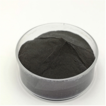
TRUNNANO is a globally recognized Molybdenum Disulfide manufacturer and supplier of compounds with more than 12 years of expertise in the highest quality nanomaterials and other chemicals. The company develops a variety of powder materials and chemicals. Provide OEM service. If you need high quality Molybdenum Disulfide, please feel free to contact us. You can click on the product to contact us.
Tags: Molybdenum Disulfide, nano molybdenum disulfide, MoS2
All articles and pictures are from the Internet. If there are any copyright issues, please contact us in time to delete.
Inquiry us